- 您现在的位置:买卖IC网 > Sheet目录368 > W9425G6EH-5 (Winbond Electronics)IC DDR-400 SDRAM 256MB 66TSSOPII
�� �
�
�W9425G6EH�
�9.5�
�DC� Characteristics�
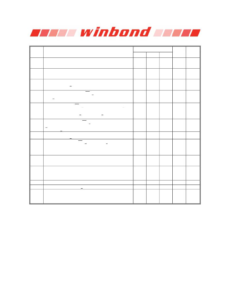
�SYM.�
�I� DD0�
�I� DD1�
�I� DD2P�
�I� DD2F�
�PARAMETER�
�Operating� current:� One� Bank� Active-Precharge;� t� RC� =� t� RC� min;�
�t� CK� =� t� CK� min;� DQ,� DM� and� DQS� inputs� changing� twice� per� clock�
�cycle;� Address� and� control� inputs� changing� once� per� clock� cycle�
�Operating� current:� One� Bank� Active-Read-Precharge;� Burst� =� 2;�
�t� RC� =� t� RC� min;� CL� =� 3;� t� CK� =� t� CK� min;� I� OUT� =� 0� mA;� Address� and�
�control� inputs� changing� once� per� clock� cycle.�
�Precharge� Power� Down� standby� current:� All� Banks� Idle;� Power�
�down� mode;� CKE� <� V� IL� max;� t� CK� =� t� CK� min;� Vin� =� V� REF� for� DQ,�
�DQS� and� DM�
�Idle� floating� standby� current:� CS� >� V� IH� min;� All� Banks� Idle;�
�CKE� >� V� IH� min;� Address� and� other� control� inputs� changing� once�
�-4�
�110�
�150�
�20�
�45�
�MAX.�
�-5/-5I�
�110�
�150�
�20�
�45�
�-6/-6I�
�110�
�150�
�20�
�45�
�UNIT�
�mA�
�NOTES�
�7�
�7,� 9�
�7�
�per� clock� cycle;� Vin� =� Vref� for� DQ,� DQS� and� DM�
�Idle� standby� current:� CS� >� V� IH� min;� All� Banks� Idle;� CKE� >� V� IH�
�I� DD2N�
�min;� t� CK� =� t� CK� min;� Address� and� other� control� inputs� changing�
�once� per� clock� cycle;� Vin� >� V� IH� min� or� Vin� <� V� IL� max� for� DQ,�
�45�
�45�
�45�
�7�
�DQS� and� DM�
�I� DD2Q�
�Idle� quiet� standby� current:� CS� >� V� IH� min;� All� Banks� Idle;� CKE�
�>� V� IH� min;� t� CK� =� t� CK� min;� Address� and� other� control� inputs�
�40�
�40�
�40�
�7�
�stable;� Vin� >� V� REF� for� DQ,� DQS� and� DM�
�I� DD3P�
�Active� Power� Down� standby� current:� One� Bank� Active;� Power�
�down� mode;� CKE� <� V� IL� max;� t� CK� =� t� CK� min�
�20�
�20�
�20�
�Active� standby� current:� CS� >� V� IH� min;� CKE� >� V� IH� min;� One�
�I� DD3N�
�Bank� Active-Precharge;� t� RC� =� t� RAS� max;� t� CK� =� t� CK� min;� DQ,� DM�
�and� DQS� inputs� changing� twice� per� clock� cycle;� Address� and�
�70�
�70�
�70�
�7�
�other� control� inputs� changing� once� per� clock� cycle�
�I� DD4R�
�Operating� current:� Burst� =� 2;� Reads;� Continuous� burst;� One�
�Bank� Active;� Address� and� control� inputs� changing� once� per�
�clock� cycle;� CL=3;� t� CK� =� t� CK� min;� I� OUT� =� 0mA�
�210�
�180�
�170�
�7,� 9�
�Operating� current:� Burst� =� 2;� Write;� Continuous� burst;� One� Bank�
�I� DD4W�
�Active;� Address� and� control� inputs� changing� once� per� clock�
�cycle;� CL� =� 3;� t� CK� =� t� CK� min;� DQ,� DM� and� DQS� inputs� changing�
�210�
�180�
�170�
�7�
�twice� per� clock� cycle�
�I� DD5�
�I� DD6�
�Auto� Refresh� current:� t� RC� =� t� RFC� min�
�Self� Refresh� current:� CKE� <� 0.2V�
�190�
�3�
�190�
�3�
�190�
�3�
�7�
�Random� Read� current:� 4� Banks� Active� Read� with� activate� every�
�I� DD7�
�20nS,� Auto-precharge� Read� every� 20� nS;� Burst� =� 4;� t� RCD� =� 3;�
�I� OUT� =� 0mA;� DQ,� DM� and� DQS� inputs� changing� twice� per� clock�
�300�
�300�
�300�
�cycle;� Address� changing� once� per� clock� cycle�
�Publication� Release� Date:Dec.� 03,� 2008�
�-� 26� -�
�Revision� A08�
�发布紧急采购,3分钟左右您将得到回复。
相关PDF资料
W9425G6JH-5I
IC DDR SDRAM 256MBIT 66TSOPII
W947D2HBJX5E
IC LPDDR SDRAM 128MBIT 90VFBGA
W948D2FBJX5E
IC LPDDR SDRAM 256MBIT 90VFBGA
W949D2CBJX5E
IC LPDDR SDRAM 512MBIT 90VFBGA
W971GG6JB25I
IC DDR2 SDRAM 1GBIT 84WBGA
W971GG8JB-25
IC DDR2 SDRAM 1GBIT 60WBGA
W9725G6IB-25
IC DDR2-800 SDRAM 256MB 84-WBGA
W9725G6JB25I
IC DDR2 SDRAM 256MBIT 84WBGA
相关代理商/技术参数
W9425G6EH-5I
制造商:Winbond Electronics Corp 功能描述:
W9425G6JB-5
制造商:Winbond Electronics Corp 功能描述:DRAM Chip DDR SDRAM 256M-Bit 16Mx16 2.5V 60-Pin TFBGA 制造商:Winbond Electronics 功能描述:IC MEMORY 制造商:Winbond Electronics Corp 功能描述:IC MEMORY 制造商:Winbond 功能描述:16MX16,256Mb DDRI DRAM ,200MHZ, BGA
W9425G6JB-5 TR
制造商:Winbond Electronics Corp 功能描述:256M DDR SDRAM X16, 200MHZ
W9425G6JB-5I
制造商:Winbond Electronics Corp 功能描述:DRAM Chip DDR SDRAM 256M-Bit 16Mx16 2.5V 制造商:Winbond Electronics 功能描述:IC MEMORY 制造商:Winbond Electronics Corp 功能描述:IC MEMORY
W9425G6JB-5I TR
制造商:Winbond Electronics Corp 功能描述:256M DDR SDRAM X16, 200MHZ, IN
W9425G6JH
制造商:WINBOND 制造商全称:Winbond 功能描述:4 M × 4 BANKS × 16 BITS DDR SDRAM
W9425G6JH-4
制造商:Winbond Electronics Corp 功能描述:DRAM Chip DDR SDRAM 256M-Bit 16Mx16 2.5V 66-Pin TSOP-II 制造商:Winbond Electronics 功能描述:IC MEMORY 制造商:Winbond Electronics Corp 功能描述:IC MEMORY 制造商:Winbond 功能描述:16MX16,256MB DDR,250MHZ,2.5V , TSOP 66PIN GREEN
W9425G6JH4TR
制造商:Winbond Electronics Corp 功能描述:256M DDR SDRAM X16, 250MHZ, 65